Specifications
Technological capabilities
Board type
SS – Single-sided printed circuit board
DS – Double-sided printed circuit board
ML – Multilayer printed circuit board
Basic material
FR4, CEM1
IMS (Al), IMS (Cu)
PTFE, RF
IZOKART (Pertinaks), VITROPLAST
Manufacturers of basic materials
Kingboard, Nanya, Isola, Rogers, Bergquist …
Thermal stability
TG130 – TG210
Thermal conductivity of IMS
0,3 W/m°C
2,0 W/m°C (standard)
5 W/m°C
Maximal work panel
500 x 600 mm
Thickness of finished PCB
0,2 mm – 3,2 mm
Thickness of inner layers
0,08 mm – 3,2 mm
Minimum line width
70 µm (70 µm)
Thickness of base copper foil
18 μm, 35 μm, 70 μm, 105 μm
Thickness of base copper foil on intermediate layers
18 μm, 35 μm, 70 μm, 105 μm
Diameter of the smallest non-bore hole
0,15 mm
Types of boreholes
Through hole
Blind vias
Buried vias
Half holes
Blind vias (depth-to-diameter ratio)
1 : 1
Solder mask
Green: matt, glossy (standard)
Black
White
Blue
Red
Yellow
Minimum gap in fine pitch
70 μm
Silk screen color
Green
Black
White
Blue
Red
Yellow
Peelable mask
EM55/4748 R-LF (Electra Polymer)
Tented via
With solder mask
Filled via
With non-conductive past,
According to IPC-4761 – 6a + 6b + 7
Surface treatment
HAL lead-free (RoHS)
Immersion Au (ENIG)
Galvanic Au (Hard gold)
Mechanical tolerance
According to DIN ISO 2768 T1
Final product thickness
+/-10 %
Etching tolerance
+/-20 % (+/-10%)
PCBA
Documentation
Well-prepared documentation is essential for a well-made product.
To make the product, we will need the following:
- GERBER files
- BILL OF MATERIALS (Excel file)
- PICK AND PLACE file
- TESTING PROTOCOL (if you require final testing of PCBs)
Electronic components
We always purchase electronic components according to their exact designations declared by the customer. If a particular component is not in stock or the supply period is extremely long, we recommend an alternative product or ask for a suggested replacement option.
Options:
- components supplied by customer
- components partly supplied by the customer and partly by LUZNAR d.o.o.
- components entirely supplied by LUZNAR d.o.o.
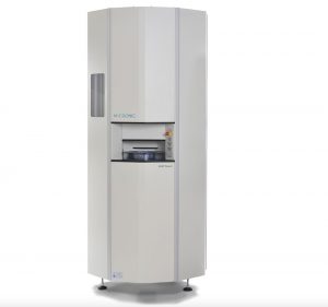
COMPONENT STORAGE TOWER
Advantages:
-
Traceability of components
-
Controlled atmosphere storage
-
Automatic component preparation

SMT printing
At LUZNAR d.o.o. we no longer use stencils to apply soldering paste on printed circuit boards. This acquisition has greatly improved the SMT component installation and reduced the costs of initial preparations.
We have added an extra printer to our wide array of equipment.

Printing specification:
- Print precision: 20 µ
- Minimum point size: 215 µ
- Minimum point volume: 5 nl
- Maximum panel size for our machine: 508×508 mm
- Circuit thickness: 50µ -> 6,0 mm
Printing advantages:
- Built-in optical paste control
- Automatic paste touch-up
- Printing of glue
- Printing of lead-free paste
- Printing of leaded paste
- Optional combined printing of adhesive and paste
- Replacing the product for assembly 1 min
SMT installation
We use a world renowned brand in the field of electronic component installation. Specifically, SAMSUNG, which is distinguished by accuracy, speed and reliability. We added two new MYCRONIC electronic component installations.
This year we have incorporated two new MYCRONIC laying lines.
Installation specification:
- Speed of assembly: 54.000 components per hour
- Accuracy: ±0,01mm
- Minimum component: 01005 (0,4 x 0,2 mm)
- Maximum component: 75 x 75 mm
- Thickness of PCBs: 50µ -> 4,2 mm
- Maximal panel size for our machine: 500 x 400 mm
Installation advantages:
- Trolleys used for material: allow a fast replacement of products
- The product is replaced in 15 minutes
- Smart feeders: for component traceability
3D AOI inspection
With regard to precision, the 3D inspection technology for assembled boards is at the cutting edge. Our machine checks every single PCB passing through our assembly department. We are able to examine the accuracy of component installation by width, length, height and rotation. In addition, we also examine the inscriptions on the components to eliminate any misplaced components. At Tiskana vezja LUZNAR d.o.o., the circuit boards are also marked with serial numbers, which can help us track the errors during the production process.

SMT optical inspection:
- Camera: 15 mega Pixel
- Resolution: 10µ
- Minimum component: 01005 (0,4×0,2mm)
-
Maximum panel size for our machine: 500 x 400mm
THT insertion and wave soldering
In recent years, the THT component insertion technology has been facing a steady decline. The PCBs are becoming ever more complex and developers are increasingly avoiding the THT components, which are being replaced with SMT components. This technology is still used at LUZNAR.
Capabilities:
Functionality test
At Tiskana vezja LUZNAR d.o.o., we develop measurement protocols, testing devices and provide advice in the preparation of test protocols. We pay close attention to the inspection and calibration of PCBs, as we are well aware that our customers want circuit boards that work 100%.
Cleaning and coating of PCBs
Electronic devices are becoming more and more visible. This has led us to conclude that PCBs should have a visually appealing design. The demand for PCB cleaning grows every day and Tiskana vezja LUZNAR d.o.o. certainly follows the preferences of its customers.
The PCBs which are exposed to extreme temperatures, humidity, dust and vibrations require additional protection. We can ensure this by providing coating services, applying encapsulation materials and making sure that large components are securely attached.